In the high-stakes world of semiconductor manufacturing, the leap from a conceptual circuit to a functional silicon chip is bridged by Integrated Circuit (IC) Design and Verification tools. These specialized software platforms, collectively known as Electronic Design Automation (EDA), are the bedrock upon which modern electronics—from the smartphone in your pocket to the AI-accelerators in global data centers—are built.
The complexity of IC design has reached an inflection point. The industry is currently grappling with “Angstrom-era” nodes ($2\text{nm}$ and below), where traditional physics-based design rules are being augmented by generative AI. Verification, once a mere “check-box” step, now consumes nearly 70% of the entire design cycle. A single undetected bug can lead to a “re-spin” costing upwards of $50 million, making these tools not just productive assets, but financial insurance policies.
Real-World Use Cases
- AI & Hyperscale Computing: Designing massive NPUs (Neural Processing Units) with billions of transistors that require extreme thermal and power integrity checks.
- Automotive Safety: Ensuring that chips for autonomous driving comply with rigid safety standards like ISO 26262 to prevent hardware failures at high speeds.
- Telecommunications: Designing RF (Radio Frequency) front-ends for 5G and 6G that manage complex signal modulations without interference.
- Chiplet Architectures: Verifying 3D-IC designs where multiple dies are stacked vertically, requiring complex interconnect analysis.
What Buyers Should Evaluate
- Foundry Certification: Does the tool have “Golden” sign-off status with major foundries like TSMC, Samsung, or Intel?
- Scalability: Can the tool handle multi-billion transistor designs across distributed cloud clusters?
- AI Integration: Does it feature autonomous optimization (e.g., AI-driven place-and-route) to shorten design cycles?
- PPA Optimization: How effectively does it balance Power, Performance, and Area?
- Interoperability: Does it play well with third-party IP and other tools in the EDA ecosystem?
- Security: Does it offer encrypted design databases and secure multi-user collaboration?
Best for: Semiconductor enterprises, fabless design houses, and hardware engineering teams focusing on high-performance computing, automotive, and mobile SoCs.
Not ideal for: Pure-play software developers, basic hobbyist electronics (where simpler PCB tools suffice), or companies not involved in custom silicon manufacturing.
Key Trends in IC Design & Verification Tools
- Generative AI Design Assistants: Tools are moving from manual scripting to “agentic” AI models that can suggest RTL (Register Transfer Level) optimizations or automatically close coverage gaps.
- Cloud-Native EDA: To combat the massive compute requirements of sub-5nm nodes, vendors are offering “burst-to-cloud” capabilities, allowing teams to scale from 10 to 10,000 cores during peak verification.
- Digital Twin Verification: Hardware-software co-verification is now done via digital twins, allowing firmware teams to start their work months before a physical chip exists.
- 3D-IC and Heterogeneous Integration: A shift from monolithic chips to chiplets is driving the need for tools that can verify thermal and electrical interactions between stacked dies.
- Sustainability & Power-Aware Design: With data center energy consumption under scrutiny, tools are prioritizing “milliwatt-accurate” power analysis earlier in the design phase.
- Shift-Left Security: Verification now includes “hardware root of trust” checks to ensure no backdoors are introduced during the automated synthesis process.
- Open-Source Momentum: While the “Big Three” dominate, open-source projects like RISC-V are encouraging the use of open-source EDA components for academic and research-driven design.
- Standardized Data Models: Movement toward unified databases (like Cadence’s Unified Data Model or Synopsys’s Fusion Data Model) to prevent data loss between design stages.
How We Selected These Tools (Methodology)
To select the top 10 IC Design and Verification tools, we followed a rigorous evaluation framework:
- Market Mindshare: We prioritized tools that are “industry standard” and required by foundries for final sign-off.
- Node Support: Preference was given to tools that support advanced process nodes ($5\text{nm}$ to $2\text{nm}$ and below).
- AI Capabilities: We assessed how deeply AI is integrated into the tool’s core optimization engines.
- Verification Throughput: Tools were rated based on their ability to minimize “Time-to-Results” (TTR).
- Foundry Collaboration: We verified whether the tools are part of the certified design flows for the world’s leading semiconductor manufacturers.
- Security Posture: Evaluation of tool support for encrypted IP and secure collaboration environments.
- Ecosystem Depth: We looked for platforms that offer a “full-stack” experience—from schematic capture to physical verification.
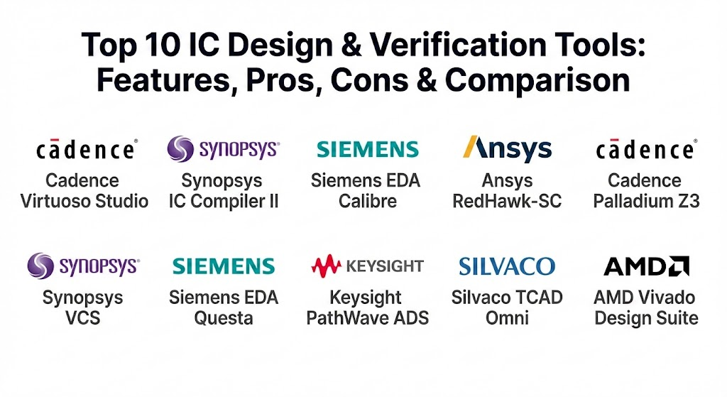
Top 10 IC Design & Verification Tools
1 — Cadence Virtuoso Studio
The industry-leading platform for custom analog, mixed-signal, and RF design. It is the definitive environment for transistor-level layout and high-precision circuitry.
Key Features
- Schematic-Driven Layout (SDL): Seamlessly translates circuit diagrams into physical silicon geometry with real-time connectivity.
- Virtuoso ADE Suite: Advanced simulation environment for analyzing circuit performance across extreme temperature and voltage corners.
- AI-Driven Layout Automation: Features like “Layout XL” automate the placement of complex transistor clusters and routing.
- Heterogeneous Integration: Supports co-design of ICs, packages, and boards in a single cockpit to manage 3D-IC complexities.
- Real-time DRC: In-design Design Rule Checking ensures engineers don’t create manufacturing errors while drawing, reducing sign-off iterations.
Pros
- Unrivaled precision for analog, high-speed, and RF design.
- Deeply integrated with almost every major semiconductor foundry’s PDK (Process Design Kit).
Cons
- Steep learning curve for junior engineers.
- Licensing costs are among the highest in the EDA industry.
Platforms / Deployment
- Linux (Red Hat / SUSE)
- Cloud / Hybrid
Security & Compliance
- ISO 27001 certified.
- Supports granular RBAC, encrypted databases, and multi-factor authentication (MFA).
Integrations & Ecosystem
Virtuoso sits at the center of the Cadence ecosystem, integrating tightly with sign-off and simulation engines:
- Cadence Spectre (Circuit Simulation)
- Cadence Quantus (Parasitic Extraction)
- Cadence Pegasus (Physical Verification)
Support & Community
Extensive. Cadence provides a massive Online Support portal, structured training, and a global “Cadence Live” community series with deep technical forums.
2 — Synopsys IC Compiler II
A high-performance digital implementation (Place-and-Route) tool designed to close the most complex SoCs with optimal Power, Performance, and Area (PPA).
Key Features
- DSO.ai Integration: Uses reinforcement learning to autonomously explore design spaces for better PPA outcomes.
- Native Multi-Voltage Support: Optimizes power across multiple voltage domains automatically to preserve battery life.
- Hierarchical Design: Handles multi-billion gate designs by breaking them into manageable blocks without losing top-level context.
- Advanced Clock Tree Synthesis (CTS): Ensures perfectly timed signals across massive chip surfaces at sub-nanosecond precision.
- Cloud-Optimized Architecture: Utilizes distributed processing for significantly faster turnaround times on massive designs.
Pros
- Exceptional at handling “impossible” timing closure on advanced nodes ($3\text{nm}$ and $2\text{nm}$).
- The AI-driven DSO.ai feature significantly reduces the number of human iterations needed for floorplanning.
Cons
- Requires significant compute hardware (massive RAM) for top-level chip closure.
- Highly complex scripting environment (primarily Tcl-based).
Platforms / Deployment
- Linux
- Cloud-native (Synopsys Cloud)
Security & Compliance
- SOC 2 Type II compliant.
- Features “Secure Design Environment” (SDE) for military-grade IP protection.
Integrations & Ecosystem
Seamlessly works with the Synopsys “Fusion” platform for a unified data model:
- Synopsys Design Compiler (Logic Synthesis)
- Synopsys PrimeTime (Static Timing Analysis)
- Synopsys Star-RC (Extraction)
Support & Community
Excellent. Synopsys SolvNetPlus is a premier knowledge base with deep technical whitepapers and an extensive network of application engineers.
3 — Siemens EDA Calibre
The “Golden” sign-off tool for physical verification. If a design passes Calibre, foundries generally guarantee it can be manufactured.
Key Features
- nmDRC: The industry standard for Design Rule Checking at nanometer scales.
- nmLVS: Validates that the physical layout matches the electrical schematic (Layout vs. Schematic).
- Extraction (PEX): Accurately models parasitic resistance and capacitance to ensure timing accuracy.
- Calibre PERC: Checks for reliability issues like Electrostatic Discharge (ESD) and electrical overstress.
- YieldEnhancer: Automatically adds “dummy metal” and optimizes geometries to improve chip manufacturing yield.
Pros
- Trusted by every major foundry; the absolute standard for final sign-off before manufacturing.
- Unmatched scalability for full-chip verification using thousands of CPU cores in parallel.
Cons
- Can be slow for very large designs if not properly partitioned or if hardware is insufficient.
- Primary focus is verification; requires other tools for the actual implementation stages.
Platforms / Deployment
- Linux
- Hybrid / Cloud
Security & Compliance
- ISO 27001 and ISO 26262 (Automotive) certified.
Integrations & Ecosystem
Integrates into every major design cockpit (Virtuoso, Innovus, IC Compiler II):
- Standard interfaces for Tcl and Python scripting.
- Direct integration with Siemens mPower for power integrity analysis.
Support & Community
Strong enterprise support with dedicated Application Engineers (AEs) for major accounts and a deep technical library.
4 — Ansys RedHawk-SC
A power integrity and reliability sign-off platform built on a big-data architecture for the most demanding SoCs and 3D-ICs.
Key Features
- Sea-of-Nodes Architecture: Allows for full-chip power analysis without needing to partition the design, ensuring no local hot spots are missed.
- Thermal-Aware EM: Checks if high temperatures will cause the chip’s wires to degrade over time (Electromigration).
- Voltage Drop Analysis: Ensures every transistor gets enough power to switch at the right speed during peak activity.
- Chip-Package-System Co-analysis: Analyzes how the package and PCB affect the chip’s power delivery network.
Pros
- The industry leader for power-integrity and thermal sign-off.
- Extremely fast due to its cloud-native, distributed computing backend.
Cons
- Niche focus (Power/Thermal); must be used alongside implementation tools like IC Compiler or Innovus.
- High resource consumption for its “big data” analytics engines.
Platforms / Deployment
- Linux
- Cloud / Self-hosted
Security & Compliance
- SOC 2 compliant.
Integrations & Ecosystem
Integrates with all major implementation flows (Synopsys, Cadence):
- Standard foundry-certified models for all major process nodes.
- Robust APIs for custom data extraction and visualization.
Support & Community
Robust. Ansys offers excellent simulation-focused webinars, technical documentation, and a global support network.
5 — Cadence Palladium Z3
An enterprise-scale hardware emulation platform that allows teams to run software on their “chip” before the physical silicon is manufactured.
Key Features
- Massive Capacity: Can emulate designs with up to 18 billion gates, suitable for the largest data center chips.
- High-Speed Compile: Turns RTL code into an emulated hardware model in hours, enabling faster iteration cycles.
- Virtual Target Interfaces: Connects the emulated chip to real-world peripherals like USB, PCIe, and Ethernet.
- Dynamic Power Analysis: Tracks power consumption while running real software workloads to find power-hungry code.
Pros
- Crucial for early software bring-up and firmware debugging, saving months of time.
- Significantly faster than software-based simulators, allowing for millions of test cycles per second.
Cons
- Requires massive, expensive physical hardware cabinets (data center scale).
- Typically only affordable for Tier-1 semiconductor companies.
Platforms / Deployment
- On-premise hardware / Cloud (Cadence Cloud)
Security & Compliance
- Varies / Not publicly stated.
Integrations & Ecosystem
Integrates with the Cadence Verification Suite:
- Cadence Protium (Prototyping)
- Cadence Jasper (Formal Verification)
Support & Community
High-touch enterprise support model with dedicated onsite support for large installations.
6 — Synopsys VCS
The industry’s highest-performance functional simulation engine, used to verify the logical correctness of digital designs.
Key Features
- Fine-Grained Parallelism: Distributes simulation tasks across multiple CPU cores to speed up large regression tests.
- UVM Support: Native, high-performance support for the Universal Verification Methodology.
- Verdi Debug Integration: The industry-standard waveform viewer for finding logical bugs in complex code.
- VSO.ai: AI-driven verification to find bugs faster and reach 100% coverage sooner by predicting where bugs hide.
Pros
- Extremely fast execution for large-scale regressions.
- Verdi debug environment is widely considered the best in the industry for visualizing complex logic.
Cons
- Can be complex to set up for multi-language (SystemVerilog/VHDL) environments.
- Licensing is tied closely to the Synopsys ecosystem for maximum performance.
Platforms / Deployment
- Linux
- Cloud / Hybrid
Security & Compliance
- ISO 27001 compliant.
Integrations & Ecosystem
Part of the Synopsys Verification Continuum:
- Synopsys ZeBu (Emulation)
- Synopsys SpyGlass (Linting and CDC analysis)
Support & Community
Extensive documentation and a large user base across global design centers.
7 — Siemens EDA Questa
A comprehensive functional verification platform that combines simulation, formal verification, and hardware-software co-verification.
Key Features
- Unified Coverage Database: Consolidates results from simulation, formal, and emulation in one place for easier reporting.
- Questa Formal: Uses mathematical proofs to find “corner case” bugs that random simulation might miss.
- Power-Aware Simulation: Verifies that low-power states (sleep/wake) don’t break the chip’s logic.
- Visualizer Debug: High-performance debug environment with automated “cause-and-effect” analysis for faster bug fixing.
Pros
- Excellent formal verification capabilities that are relatively easy to use.
- Strong support for mixed-language and high-level synthesis (C/C++) flows.
Cons
- The UI can feel dated compared to newer “Studio” type integrated environments.
- Integration with non-Siemens implementation tools can require extra effort for seamless data transfer.
Platforms / Deployment
- Windows / Linux
- Cloud / Self-hosted
Security & Compliance
- Not publicly stated.
Integrations & Ecosystem
Integrates with Siemens Veloce (Emulation) and Siemens Tessent (Design-for-Test) platforms.
Support & Community
Strong academic presence; many engineers learn verification on Questa or its predecessor, ModelSim.
8 — Keysight PathWave ADS
The gold standard for RF, microwave, and high-speed digital design, essential for wireless communication and radar chips.
Key Features
- Electromagnetic (EM) Simulation: Analyzes how high-frequency signals radiate and interfere within the chip package.
- Signal Integrity Analysis: Critical for high-speed interfaces like DDR5, DDR6, and PCIe Gen6/7.
- Circuit-System Co-simulation: Simulates the entire radio chain from the antenna to the digital baseband.
- WINS (Wireless Insite): Models how chips perform in complex, real-world wireless environments.
Pros
- The specialized tool for 5G, 6G, and satellite communications.
- Highly accurate device models for modern materials like Gallium Nitride (GaN).
Cons
- Very specialized; not suitable for general-purpose digital logic or CPUs.
- High hardware requirements for complex 3D EM simulations.
Platforms / Deployment
- Windows / Linux
- On-premise
Security & Compliance
- ISO 27001 compliant.
Integrations & Ecosystem
Integrates with Cadence Virtuoso for high-performance RFIC flows.
- Supports standard data formats for vector signal analysis.
Support & Community
Keysight offers world-class technical support and extensive “How-To” video libraries and application notes.
9 — Silvaco TCAD Omni
Technology Computer-Aided Design (TCAD) software used to simulate the actual physical manufacturing and electrical behavior of semiconductor devices.
Key Features
- Process Simulation: Models etching, deposition, and implantation of silicon at the atomic level.
- Device Simulation: Predicts the electrical behavior of a single transistor before it’s even built.
- Advanced Material Support: Simulation for new materials like perovskites, SiC, and carbon nanotubes.
- Machine Learning Optimization: Automatically tunes process parameters to achieve target performance without physical experiments.
Pros
- Essential for R&D and foundries developing the next generation of process nodes.
- Strong at modeling physical effects that occur at the atomic level.
Cons
- Not a design tool for chip architects; this is for device physicists and process engineers.
- Extremely high learning curve involving advanced physics and chemistry.
Platforms / Deployment
- Linux
- Self-hosted
Security & Compliance
- Not publicly stated.
Integrations & Ecosystem
Outputs device models (SPICE models) that are then used by circuit designers in tools like Virtuoso.
Support & Community
Niche but highly expert community; strong relationship with research universities and global foundries.
10 — AMD Vivado Design Suite
The standard design environment for AMD (Xilinx) FPGAs and Adaptive SoCs, focusing on hardware acceleration and programmable logic.
Key Features
- IP Integrator: Graphical environment for building complex systems using pre-verified IP blocks.
- High-Level Synthesis (HLS): Allows engineers to write hardware logic in C or C++ instead of Verilog/VHDL.
- AI Engine Support: Specialized tools for programming and simulating AMD’s dedicated AI-accelerator blocks.
- Hardware Debugging: Integrated logic analyzer for real-time, on-chip debugging of the running design.
Pros
- The best-in-class tool for FPGA developers, offering a very modern user interface.
- Massive library of pre-verified IP blocks for everything from Ethernet to memory controllers.
Cons
- Proprietary; only works for AMD/Xilinx hardware.
- Compile times for very large FPGAs can take several hours on standard workstations.
Platforms / Deployment
- Windows / Linux
- Desktop / Cloud
Security & Compliance
- SOC 2 compliant.
- Supports bitstream encryption and hardware Root of Trust for secure field updates.
Integrations & Ecosystem
Integrates with AMD Vitis for unified software-hardware development and acceleration.
Support & Community
One of the largest and most active hardware communities in the world via the Xilinx/AMD Forums.
Comparison Table
| Tool Name | Best For | Platform(s) | Deployment | Standout Feature | Public Rating |
| Cadence Virtuoso | Analog/RF Design | Linux | Hybrid | Transistor-level precision | N/A |
| Synopsys IC Comp II | Digital Implementation | Linux | Cloud-native | DSO.ai (AI Optimization) | N/A |
| Siemens Calibre | Physical Sign-off | Linux | Hybrid | “Golden” Foundry Status | N/A |
| Ansys RedHawk-SC | Power Integrity | Linux | Cloud | Big-data power analytics | N/A |
| Cadence Palladium | Emulation/FW Boot | Hardware | On-prem/Cloud | Hardware-speed simulation | N/A |
| Synopsys VCS | Digital Simulation | Linux | Cloud | VSO.ai (AI Verification) | N/A |
| Siemens Questa | Functional Verification | Windows/Linux | Hybrid | Formal Verification | N/A |
| Keysight ADS | RF/Microwave Design | Windows/Linux | On-prem | High-frequency EM Sim | N/A |
| Silvaco TCAD | Device Physics/R&D | Linux | Self-hosted | Atomic-level process sim | N/A |
| AMD Vivado | FPGA/Adaptive SoC | Windows/Linux | Hybrid | IP-centric Design Flow | N/A |
Evaluation & Scoring
| Tool Name | Core (25%) | Ease (15%) | Integrations (15%) | Security (10%) | Performance (10%) | Support (10%) | Value (15%) | Weighted Total |
| Cadence Virtuoso | 10 | 5 | 10 | 9 | 9 | 10 | 6 | 8.40 |
| Synopsys IC Comp II | 10 | 6 | 10 | 9 | 10 | 9 | 6 | 8.45 |
| Siemens Calibre | 10 | 6 | 9 | 9 | 10 | 9 | 7 | 8.55 |
| Ansys RedHawk-SC | 9 | 7 | 8 | 9 | 10 | 8 | 7 | 8.25 |
| Cadence Palladium | 10 | 4 | 9 | 8 | 10 | 9 | 4 | 7.75 |
| Synopsys VCS | 10 | 7 | 9 | 9 | 10 | 9 | 7 | 8.65 |
| Siemens Questa | 9 | 7 | 8 | 8 | 9 | 8 | 8 | 8.25 |
| Keysight ADS | 10 | 6 | 7 | 9 | 9 | 9 | 7 | 8.25 |
| Silvaco TCAD | 9 | 4 | 6 | 7 | 8 | 8 | 7 | 7.15 |
| AMD Vivado | 9 | 8 | 7 | 9 | 8 | 10 | 9 | 8.60 |
How to Interpret These Scores:
- Core (25%): Technical capability and breadth of features in its specific niche.
- Ease (15%): How quickly a new engineer can become productive.
- Weighted Total: A comparative average where “10” represents the absolute market leader in that specific category.
Which Tool Is Right for You?
Solo / Freelancer
For independent contractors or students, heavy enterprise suites are cost-prohibitive.
- Recommendation: Look into AMD Vivado (Web Edition is free) for FPGA-based learning, or open-source tools like Verilator or KiCad for less complex projects.
SMB / Startups
Startups need to balance “sign-off” quality with limited budgets.
- Recommendation: Use a “pay-per-use” cloud model via Synopsys Cloud or Cadence OnCloud. This allows access to top-tier tools without the $100k+ upfront perpetual license cost.
Mid-Market
Companies with established product lines (e.g., IoT, specialized sensors).
- Recommendation: A mixed-vendor flow often works best here. Siemens Questa for verification and Ansys RedHawk-SC for power can be combined with a primary implementation suite for a balanced TCO.
Enterprise
Tier-1 semiconductor firms (Apple, NVIDIA, Qualcomm).
- Recommendation: Full-stack suites from Cadence or Synopsys are mandatory. These organizations prioritize Cadence Palladium for emulation and Synopsys DSO.ai for productivity, as time-to-market is more critical than license cost.
Frequently Asked Questions (FAQs)
1.What is the average price of an EDA tool license?
Pricing is rarely public, but a single “seat” for a high-end sign-off tool can range from $50,000 to $250,000 per year. Enterprise agreements for full suites can reach tens of millions of dollars.
2.Can these tools run on a standard laptop?
Generally, no. Most IC design tools require powerful Linux servers with 128GB to 2TB of RAM and high-speed network storage to handle the massive data volumes.
3.Is AI actually helping in IC design?
Yes. AI-driven tools like DSO.ai are now used in production. They can reduce the time taken to find an optimal chip layout from weeks of human “tweaking” to just a few days of automated exploration.
4.What is a PDK and why does it matter?
A Process Design Kit (PDK) is a set of files from the foundry (e.g., TSMC) containing physical and electrical rules for a specific manufacturing node. Without the PDK, these tools cannot generate manufacturable designs.
5.What is “Tapeout”?
“Tapeout” is the final stage where the design database is sent to the foundry for manufacturing. It is the culmination of months of verification to ensure zero errors.
6.Why is Linux the standard for EDA?
Linux offers superior memory management and stability for long-running simulations (which can take weeks) and better scripting capabilities compared to other operating systems.
7.Can I learn these tools for free?
Most vendors offer “University Programs” or student editions. Additionally, learning SystemVerilog and Python is a great way to prepare for the automation side of these tools.
8.What is the difference between Simulation and Emulation?
Simulation is software-based and runs on general CPUs (slower but cheap). Emulation uses specialized hardware (like Palladium) to mimic the chip, making it thousands of times faster.
9.Do these tools support 3D-IC design?
Yes, modern versions of Virtuoso and IC Compiler II have dedicated features for managing “Through-Silicon Vias” (TSVs) and analyzing the heat generated by stacked dies.
10.Are there open-source alternatives?
Yes, projects like OpenROAD and Magic VLSI exist. While they are not yet used for high-end CPU design, they are increasingly popular for IoT and academic research.
Conclusion
The selection of an IC Design & Verification tool is one of the most consequential decisions a hardware team will make. The “best” tool is no longer just the one with the most features, but the one that integrates most effectively with AI-driven automation and cloud-scale compute. For most enterprises, the choice will revolve around the “Big Three”—Cadence, Synopsys, and Siemens—due to their deep foundry partnerships. However, specialized players like Ansys and Keysight remain irreplaceable for power and RF.
Best Cardiac Hospitals Near You
Discover top heart hospitals, cardiology centers & cardiac care services by city.
Advanced Heart Care • Trusted Hospitals • Expert Teams
View Best Hospitals