Introduction
Semiconductor yield management software is a specialized category of industrial analytics designed to help microchip manufacturers increase the percentage of functional chips produced on a single wafer. In an industry where a 1% increase in yield can translate to hundreds of millions of dollars in additional revenue, these tools are indispensable. They function by ingesting massive volumes of data from various stages of the manufacturing process—including design, wafer fabrication, assembly, and final testing—to identify “yield killers” or systematic defects that impede production.
The complexity of semiconductor manufacturing has reached an all-time high. The shift toward sub-2nm process nodes, 3D gate architectures (GAA), and heterogeneous integration through chiplets has made traditional manual analysis impossible. Modern yield management systems now leverage artificial intelligence and high-performance data pipelines to provide real-time visibility into the cleanroom. By correlating electrical test results with physical defect maps from earlier in the process, these tools allow engineers to pinpoint the exact machine or process step causing a failure before an entire batch of wafers is compromised.
Real-World Use Cases
- Excursion Detection: Automatically spotting abnormal yield drops in real-time to stop a production line before more wafers are processed incorrectly.
- Root-Cause Analysis: Correlating “bin sort” data from final testing with “metrology” data from the fab to find the specific chamber or tool responsible for a defect.
- New Product Introduction (NPI): Accelerating the “yield ramp” of a new chip design by identifying and fixing design-for-manufacturability issues in weeks rather than months.
- Advanced Packaging Traceability: Tracking individual die-level performance across complex 3D stacks to ensure that one bad chiplet doesn’t ruin an expensive high-end processor.
- Supplier Quality Management: Using yield data to hold silicon wafer suppliers or outsourced assembly and test (OSAT) partners accountable for material quality.
Evaluation Criteria for Buyers
- Data Ingestion Speed: Can the software process terabytes of data from high-volume manufacturing without lagging?
- Cross-Domain Correlation: Does it seamlessly link design (GDSII/OASIS) with manufacturing and test data?
- AI & Machine Learning: Are there built-in models for automated defect classification or predictive yield modeling?
- Deployment Model: Does the vendor support on-premises installations for high-security fabs or cloud-based platforms for fabless collaboration?
- Scalability: Is the database architecture capable of storing and searching years of historical production data?
- User Interface: Is the platform intuitive for process engineers, or does it require a dedicated data scientist to operate?
Best for: Integrated Device Manufacturers (IDMs), major foundries (fabs), and large fabless semiconductor companies that need to manage high-volume, high-complexity production across multiple global sites.
Not ideal for: Small R&D labs with low-volume prototyping, or generic manufacturing sectors that do not deal with the extreme precision and data density of microchip fabrication.
Key Trends in Semiconductor Yield Management Software
- AI-Driven Defect Classification: Using deep learning to automatically identify the “signature” of a defect on a wafer map, such as scratches or ring patterns, without human intervention.
- Layout-Aware Diagnostics: Integrating the original chip design files directly into the yield analysis to see if a specific circuit geometry is more prone to failure.
- Digital Twin Synchronization: Creating a virtual replica of the fab floor that updates in real-time based on yield data to predict how process changes will impact the final output.
- Edge-to-Cloud Analytics: Performing initial data cleaning and anomaly detection at the equipment level (edge) before sending summarized insights to a centralized cloud platform.
- Heterogeneous Integration Tracking: Specialized modules designed to track the yield of chiplets and interposers in advanced packaging, which is critical for AI and high-performance computing.
- Sustainability & Energy Monitoring: Correlating yield loss with power consumption and chemical usage to optimize for “green” manufacturing targets.
- Shift to Proactive Corrections: Moving from “detecting” failures to “predicting” them by monitoring tool health and process drift before yield actually drops.
- Universal Scene Description Adoption: Using standardized data formats to allow yield management tools to communicate more effectively with CAD and metrology equipment.
How We Selected These Tools
- Global Market Presence: We prioritized tools used by the “Big Three” foundries and major global IDMs.
- Technical Depth: Preference was given to software that handles the entire “cradle-to-grave” lifecycle from design to final test.
- AI Integration: Evaluation included the sophistication of the vendor’s machine learning and automated root-cause analysis capabilities.
- Interoperability: We looked for platforms that support standard industry data formats like STDF, ATDF, and GDSII.
- Security Posture: Given the sensitive nature of chip IP, we selected vendors with robust enterprise security and on-premises deployment options.
- Industry Reputation: Inclusion was based on long-term performance records and positive feedback from process and test engineers.
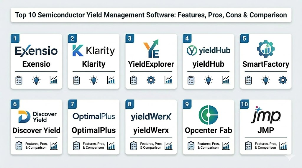
Top 10 Semiconductor Yield Management Software Tools
1. PDF Solutions Exensio
Exensio is arguably the most comprehensive yield management platform in the industry. It is designed to provide a “cradle-to-grave” view by bridging the gap between design, manufacturing, and test data across the entire semiconductor supply chain.
Key Features
- Patented C4 Yield Learning Model for physics-based attribution of yield loss.
- Comprehensive data normalization across diverse equipment types and global sites.
- Advanced analytics for advanced packaging and heterogeneous integration.
- Integrated Design-for-Manufacturability (DFM) feedback loops.
- Real-time excursion detection and automated reporting.
Pros
- Unmatched depth in correlating design intent with actual manufacturing results.
- Scalable for the world’s largest, most complex high-volume fabs.
Cons
- Extremely complex to implement and requires significant engineering resources.
- High cost of ownership makes it less accessible for smaller startups.
Platforms / Deployment
Windows / Linux
On-premises / Hybrid
Security & Compliance
Enterprise-grade SSO, MFA, and extensive audit logging for IP protection.
Not publicly stated.
Integrations & Ecosystem
Integrates deeply with all major Automatic Test Equipment (ATE) and Manufacturing Execution Systems (MES). It acts as the central data lake for semiconductor intelligence.
Support & Community
High-end enterprise support with dedicated field application engineers. It has a prestigious user community among the world’s top-tier chipmakers.
2. KLA Klarity
KLA is the dominant force in inspection and metrology equipment, and Klarity is their flagship defect management system. It excels at turning raw inspection images into actionable yield insights.
Key Features
- Automated Defect Classification (ADC) using advanced image recognition.
- Seamless integration with KLA inspection and metrology tool data.
- Spatial signature analysis to identify systematic process issues on wafers.
- High-resolution wafer mapping and defect “piling” for root-cause analysis.
- Predictive modeling for “kill ratio” estimation based on defect size and location.
Pros
- The undisputed leader for front-end defect and metrology-driven yield analysis.
- Exceptional visualization of wafer-level data and spatial patterns.
Cons
- Best performance is realized when used within a KLA-heavy equipment ecosystem.
- Can be less focused on “back-end” test data compared to some competitors.
Platforms / Deployment
Windows / Linux
On-premises
Security & Compliance
Robust local security protocols designed for high-security fab environments.
Not publicly stated.
Integrations & Ecosystem
Direct, high-speed pipelines from KLA inspection tools. It also integrates with third-party MES and SPC systems.
Support & Community
Global field application support and a comprehensive professional training portal for equipment engineers.
3. Synopsys YieldExplorer
YieldExplorer is a design-centric yield management tool from one of the world’s leaders in Electronic Design Automation (EDA). It focuses on identifying how design choices impact final manufacturing success.
Key Features
- Layout-aware diagnostics that link electrical failures to specific circuit structures.
- Rapid correlation of wafer sort data with physical design layers (GDSII).
- Advanced “volume diagnostics” to find systematic failures in high-volume production.
- Deep integration with Synopsys’ design-for-test (DFT) and EDA tools.
- High-performance database architecture for fast queries on large datasets.
Pros
- The best choice for finding yield issues related to complex circuit geometry.
- Strongest link between the “design house” and the “fab floor.”
Cons
- Highly technical interface that requires a background in EDA and design.
- Less emphasis on “sub-fab” or facility-level equipment monitoring.
Platforms / Deployment
Linux (Primary) / Windows
On-premises
Security & Compliance
Tight integration with corporate LDAP and secure design environments.
Not publicly stated.
Integrations & Ecosystem
Seamlessly integrated into the Synopsys Fusion Design Platform and major test data formats.
Support & Community
World-class technical support and deep integration with global EDA user groups and conferences.
4. yieldHub
yieldHub is a modern, cloud-native yield management system that has gained massive popularity among fabless companies and OSATs for its ease of use and collaborative features.
Key Features
- Browser-based interface that allows for global collaboration without local installs.
- Automated daily reports and instant notifications for yield excursions.
- Advanced outlier detection and die-level traceability.
- Simplified data cleansing and normalization for messy test data.
- Interactive wafer maps and trend charts accessible via mobile devices.
Pros
- Extremely fast to deploy and much easier to learn than traditional enterprise tools.
- High value for fabless companies managing multiple manufacturing partners.
Cons
- Historically perceived as more “back-end” focused, though this is changing.
- Cloud-first model may face resistance in the most conservative “air-gapped” fabs.
Platforms / Deployment
Web-based (Any OS)
Cloud / On-premises
Security & Compliance
SOC 2 compliant with robust encryption at rest and in transit.
ISO 27001 certified.
Integrations & Ecosystem
Strong support for all major STDF and ATE formats with easy API-based data ingestion.
Support & Community
High-touch customer success teams and a growing library of video-based learning resources.
5. Applied Materials SmartFactory Yield
Applied Materials is a leader in fab equipment, and their SmartFactory suite provides an integrated factory automation and yield monitoring solution that is deeply embedded in the fab’s operation.
Key Features
- Real-time Advanced Process Control (APC) for immediate machine adjustments.
- Integrated yield analysis within a broader Manufacturing Execution System (MES).
- AI-driven pattern recognition for identifying process drift.
- Comprehensive “genealogy” tracking from the wafer to the final packaged part.
- Unified source of truth for all fab data sources (WIP, FDC, Metrology).
Pros
- Deep integration with the actual machines performing the manufacturing.
- Excellent for real-time proactive corrections and fab-wide automation.
Cons
- Most effective as part of a total Applied Materials software and equipment stack.
- Can be “heavy” for companies only looking for a standalone analysis tool.
Platforms / Deployment
Windows / Linux
On-premises
Security & Compliance
Enterprise-grade identity management and secure internal data handling.
Not publicly stated.
Integrations & Ecosystem
Built to work seamlessly with the Applied Materials equipment and automation portfolio.
Support & Community
Extensive global service infrastructure and high-level professional service engagements.
6. Onto Innovation Discover Yield
Discover Yield is an enterprise-wide platform that focuses on combining parametric, defect, and yield optimization across the entire value chain, from bare wafers to packaging.
Key Features
- Multivariate analysis of variance (MANOVA) for complex variable examination.
- Unique database architecture designed for long-term product genealogy.
- Automated reporting and workflow development for rapid root-cause analysis.
- Specialized algorithms for identifying spatial anomalies and process sequences.
- Integration of “in-line” metrology with “end-of-line” test results.
Pros
- Strong focus on “value chain” predictive analytics and long-term data mining.
- Versatile across various semiconductor markets (Memory, Logic, Specialty).
Cons
- Interface can be less modern than some cloud-native competitors.
- Requires significant setup to realize its full multivariate analysis potential.
Platforms / Deployment
Windows / Linux
On-premises / Hybrid
Security & Compliance
Standard corporate security and access controls for manufacturing environments.
Not publicly stated.
Integrations & Ecosystem
Connects to various metrology and inspection data streams, with a focus on holistic fab data.
Support & Community
Professional support focused on technical engineering teams and industrial process control.
7. NI (National Instruments) OptimalPlus
Acquired by NI, OptimalPlus is a heavy-hitter in big data analytics for the semiconductor supply chain, focusing on high-volume data ingestion and real-time decision making.
Key Features
- Real-time test time optimization and outlier detection during the test process.
- Cross-site data correlation for global manufacturing networks.
- Advanced “Adaptive Test” features that change test flows based on yield patterns.
- High-volume data processing engine designed for massive daily test logs.
- Machine learning models for predicting chip reliability and field failures.
Pros
- Exceptional for high-volume manufacturing (HVM) where test time is money.
- Strongest capability for real-time “active” yield management during testing.
Cons
- Primarily focused on the “test” side of the house rather than the “fab” side.
- Complex licensing models that can scale quickly with data volume.
Platforms / Deployment
Windows / Linux
On-premises / Hybrid
Security & Compliance
High-security data silos for protecting multi-customer OSAT environments.
Not publicly stated.
Integrations & Ecosystem
Tight integration with NI test hardware and all major third-party ATE systems.
Support & Community
Professional engineering support with a strong focus on test floor efficiency and ROI.
8. yieldWerx
yieldWerx is an enterprise-grade yield analytics solution designed for both IDMs and fabless companies. It offers a balanced approach to wafer-level and package-level data analysis.
Key Features
- Robust wafer map and binning analysis for rapid yield characterization.
- Automated data loading from multiple sub-contractors and OSATs.
- High-speed parametric analysis and correlation across different test stages.
- Flexible dashboarding for engineering, management, and executive views.
- Custom “modules” for different manufacturing stages (Sort, Assembly, Final Test).
Pros
- Very engineer-friendly with a focus on day-to-day troubleshooting tasks.
- Solid balance between feature depth and speed of implementation.
Cons
- May lack some of the advanced AI “fluff” found in newer market entrants.
- Visualization tools are functional but not as visually polished as some modern suites.
Platforms / Deployment
Windows / Web
On-premises / Cloud
Security & Compliance
SSO, SOC 2 compliance, and encrypted communication protocols.
Not publicly stated.
Integrations & Ecosystem
Well-connected to the standard semiconductor data ecosystem and common database formats.
Support & Community
Strong technical support with a reputation for helping customers with complex data mapping.
9. Siemens Opcenter Execution Fab
Part of the broader Siemens industrial software portfolio, this tool integrates high-level yield analytics directly into a world-class Manufacturing Execution System (MES).
Key Features
- Deep integration with shop-floor process control and lot tracking.
- Advanced statistical process control (SPC) and automated out-of-control action plans.
- Cross-fab data harmonization for global enterprise manufacturing.
- High-fidelity digital twin integration for process simulation.
- Real-time monitoring of equipment health and its impact on product yield.
Pros
- The best choice for large enterprises that want yield integrated with their MES.
- Backed by the massive global support and reliability of the Siemens ecosystem.
Cons
- Implementation is often a multi-year, multi-million dollar project.
- Can be “too much software” for companies that only need yield analysis.
Platforms / Deployment
Windows / Linux
On-premises / Hybrid
Security & Compliance
Industry-leading enterprise security and multi-layered access controls.
Not publicly stated.
Integrations & Ecosystem
Integrates with the entire Siemens Xcelerator portfolio and major third-party ERPs.
Support & Community
Global 24/7 professional support and a massive ecosystem of industrial consultants.
10. JMP (by SAS)
While JMP is a general statistical discovery tool, it is the unofficial “standard” in many fabs for interactive data exploration, modeling, and wafer map visualization.
Key Features
- Exceptional interactive data visualization (Graph Builder) for engineers.
- Robust statistical tools for Design of Experiments (DOE) and regression.
- Specialized “Wafer Map” and “Spatial” analysis add-ins.
- Powerful scripting language (JSL) for automating complex yield reports.
- Drag-and-drop interface that is accessible to non-programmers.
Pros
- The “Swiss Army Knife” of yield analysis that almost every fab engineer already knows.
- Unbeatable for “ad-hoc” investigation and interactive data discovery.
Cons
- Not a “system of record” for managing a global fab’s data pipeline.
- Requires manual data loading or custom scripts to connect to live fab feeds.
Platforms / Deployment
Windows / macOS
Local
Security & Compliance
Standard local software security and licensing.
Not publicly stated.
Integrations & Ecosystem
Works alongside all major database and CSV-based data exports.
Support & Community
Enormous community of statistical users and a massive library of books and training.
Comparison Table
| Tool Name | Best For | Platform(s) Supported | Deployment | Standout Feature | Public Rating |
| 1. Exensio | Full Supply Chain | Windows, Linux | Hybrid | Cradle-to-Grave Traceability | N/A |
| 2. Klarity | Front-End Defect | Windows, Linux | On-premises | Defect Classification | N/A |
| 3. YieldExplorer | Design-to-Yield | Linux, Windows | On-premises | Layout Diagnostics | N/A |
| 4. yieldHub | Fabless / OSATs | Web-based | Cloud/On-prem | Browser Collaboration | N/A |
| 5. SmartFactory | Real-Time Fab | Windows, Linux | On-premises | Active Process Control | N/A |
| 6. Discover Yield | Value Chain | Windows, Linux | Hybrid | Multivariate Analysis | N/A |
| 7. OptimalPlus | High Volume Test | Windows, Linux | Hybrid | Adaptive Testing | N/A |
| 8. yieldWerx | Engineering Teams | Windows, Web | Cloud/On-prem | Wafer/Bin Analysis | N/A |
| 9. Opcenter Fab | Large Enterprise | Windows, Linux | Hybrid | MES Integration | N/A |
| 10. JMP | Ad-hoc Discovery | Windows, macOS | Local | Interactive Viz | N/A |
Evaluation & Scoring
| Tool Name | Core (25%) | Ease (15%) | Integrations (15%) | Security (10%) | Perf (10%) | Support (10%) | Value (15%) | Total |
| 1. Exensio | 10 | 4 | 10 | 9 | 10 | 9 | 5 | 8.20 |
| 2. Klarity | 9 | 6 | 8 | 8 | 10 | 9 | 6 | 8.05 |
| 3. YieldExplorer | 9 | 5 | 9 | 8 | 9 | 8 | 6 | 7.75 |
| 4. yieldHub | 7 | 10 | 9 | 9 | 8 | 9 | 10 | 8.55 |
| 5. SmartFactory | 9 | 5 | 9 | 8 | 9 | 8 | 6 | 7.75 |
| 6. Discover Yield | 8 | 7 | 8 | 8 | 9 | 8 | 7 | 7.80 |
| 7. OptimalPlus | 9 | 6 | 9 | 8 | 10 | 8 | 7 | 8.15 |
| 8. yieldWerx | 8 | 8 | 8 | 8 | 8 | 8 | 8 | 8.00 |
| 9. Opcenter Fab | 9 | 4 | 10 | 9 | 9 | 9 | 5 | 7.75 |
| 10. JMP | 6 | 9 | 6 | 5 | 9 | 10 | 9 | 7.40 |
The weighted scoring above highlights a significant shift landscape. While enterprise heavyweights like PDF Solutions (Exensio) remain the gold standard for depth, cloud-native platforms like yieldHub are scoring higher on “Total” because they address the modern need for speed, ease of use, and collaborative value across the supply chain. These scores are comparative: a tool like JMP is essential for any individual engineer, but it scores lower on “Core” because it isn’t an automated, enterprise-wide yield management system of record.
Which Semiconductor Yield Management Software Tool Is Right for You?
Solo / Freelancer
If you are a consulting engineer or working in a small design house, JMP is your primary tool. Its ability to quickly open a data file and visually find the problem is unparalleled. For small-scale test data analysis, yieldHub offers the most accessible entry point without requiring a massive hardware investment.
SMB
Small to mid-size fabless companies should prioritize yieldHub or yieldWerx. These platforms are designed for teams that need to collaborate with multiple OSATs and foundries without having a massive IT department to manage a complex on-premises server stack.
Mid-Market
For growing IDMs or larger fabless firms, Onto Innovation Discover Yield or OptimalPlus provide a good balance. They offer deeper multivariate analysis and supply-chain-wide tracking that is necessary as production volumes scale into the millions.
Enterprise
At the enterprise level—where you are running 2nm nodes or high-volume memory fabs—PDF Solutions Exensio or Siemens Opcenter are the primary candidates. These tools provide the necessary governance, cross-site synchronization, and deep design-to-test correlation required for leading-edge manufacturing.
Budget vs Premium
- Budget: yieldHub or JMP (standard license) provide high utility for a lower relative cost.
- Premium: Exensio and KLA Klarity are premium investments that require significant capital but provide the deepest “yield learning” capabilities.
Feature Depth vs Ease of Use
- Feature Depth: Houdini-like depth can be found in Synopsys YieldExplorer and Exensio; they can do anything, but they are hard to master.
- Ease of Use: yieldHub and JMP prioritize the user experience and speed to insight.
Integrations & Scalability
For companies that need to manage a global footprint of dozens of fabs and test houses, the scalability of OptimalPlus and Exensio is unmatched. They are designed to ingest and harmonize disparate data streams at a massive scale.
Security & Compliance Needs
If you are operating a high-security captive fab for government or automotive clients, Applied Materials SmartFactory or KLA Klarity are designed for the “air-gapped,” on-premises security requirements typical of these environments.
Frequently Asked Questions (FAQs)
1. What is the difference between an MES and a YMS?
An MES (Manufacturing Execution System) tracks the physical movement and history of lots in a fab, while a YMS (Yield Management System) analyzes the data produced by those lots to find the root causes of failure.
2. Why is “Design-to-Yield” correlation so important now?
At advanced nodes, failures are often caused by the specific way a circuit is designed. Linking the design files (GDSII) with test results allows engineers to see if a design rule is too tight for the fab’s capabilities.
3. Can these tools handle data from different equipment vendors?
Yes, modern yield management systems are designed to normalize data from hundreds of different tool types (lithography, etch, ATE) into a single, searchable format.
4. How long does it take to implement an enterprise YMS?
Implementation can range from a few weeks for a cloud-native tool like yieldHub to 12-18 months for a full enterprise rollout of Exensio or Siemens Opcenter.
5. What is “STDF” and why does it matter?
Standard Test Data Format (STDF) is the industry standard for logging semiconductor test results. Almost every YMS must be able to ingest this format natively.
6. Do these tools use AI for anything besides defect images?
Yes, AI is used for predictive maintenance on fab tools, identifying complex multivariate drifts in process parameters, and optimizing test flows to save time.
7. Can fabless companies use these tools without owning a fab?
Absolutely. Many fabless companies use YMS platforms to pull data from their foundry and OSAT partners to monitor quality and accelerate product launches.
8. What is a “Yield Excursion”?
An excursion is a sudden, abnormal drop in yield. A YMS is critical for detecting these immediately and identifying the “excursion source” to prevent further losses.
9. How does advanced packaging impact yield management?
Advanced packaging involves stacking multiple chips. If one chiplet in a stack of four is bad, you lose all four. Yield tools must now track individual “good die” through the entire assembly process.
10. Do I need a data scientist to run this software?
While many of these tools are becoming more “self-service” for engineers, having a team that understands statistical process control (SPC) and data modeling is highly recommended for enterprise-scale systems.
Conclusion
In the high-stakes environment semiconductor manufacturing, the difference between market leadership and financial loss often comes down to the efficiency of your yield management strategy. The shift toward sub-2nm nodes and 3D packaging has made the “invisible” data between process steps more critical than ever. Choosing the right tool depends on your position in the value chain—whether you are a design-focused fabless firm needing cloud collaboration or a high-volume IDM requiring deep on-premises process control. By investing in a system that provides real-time, actionable insights, manufacturers can transform raw data into a sustainable competitive advantage and faster time-to-market.
Best Cardiac Hospitals Near You
Discover top heart hospitals, cardiology centers & cardiac care services by city.
Advanced Heart Care • Trusted Hospitals • Expert Teams
View Best Hospitals